Nintendo Switch Hybrid Console Teardown Exposes NVIDIA Tegra Heart
We are not sure of the authenticity of this one, but over at one of Baido's Chinese-language web forums is a teardown of Nintendo's not-yet-released Switch console. If it turns out to be fake, then someone put a lot of time and effort to make it appear otherwise, as the part selection lines up with what Nintendo has revealed about the Switch. The cramped layout looks legitimate to us as well.
It is also possible that these naked shots reflect a prototype design and not the final console. Either way, it's an interesting view of the system's guts.
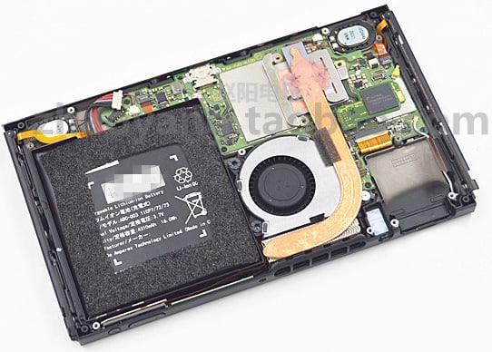
The first thing that stands out is the 4,130 mAh lithium-ion battery. It takes up nearly half of the visible area inside and sits on the right side (when viewing the display) where the power button and volume rocker are located. Size matters here because Nintendo confirmed that the battery is not user replaceable. That news came as somewhat of a buzz kill considering the console is at least equal parts mobile, if not more so. Nintendo's claim is that battery life will range from 2.5 hours to 6.5 hours.
There appears to be some foam around the battery. This is worth noting because lithium-ion batteries are sensitive to damage. One of the reasons why these types of batteries can overheat and catch fire because is because they've been dropped or otherwise banged up. The foam packing should help in that regard.

The real money shot here is of the custom NVIDIA Tegra system-on-chip (SoC) that powers the Switch. Nintendo and NVIDIA have been tight lipped about the specs of this Tegra part, leaving us to speculate.
Here is a closeup view:
When zoomed in close we can see the part number labeled as UDNX02-A2. There are a couple of things to note here. One is the "NX" designation, which is the Switch's codename, and the other is the A2 designation. Some of the speculation surrounding the Switch is that the Tegra part would be similar to the Tegra X1 chip found in NVIDIA's Shield devices, but the A2 marking as opposed to A1 found on those SoCs suggests this one is either completely different or a revised version. Best case scenario would be if NVIDIA built this around its Pascal architecture.
We'll wrap things up with an underside shot of the Switch's L-shaped circuit board. The Switch features 4GB of RAM, though it's not clear if Nintendo equipped it with a single module or two. Other specs include a 6.2-inch display with a 1280x720 resolution (can output at 1920x1080 at 60 frames per second when docked), 32GB of built-in storage, and a microSD card reader.
The Nintendo Switch is available to pre-order now for $300. It comes out March 3, 2017.
It is also possible that these naked shots reflect a prototype design and not the final console. Either way, it's an interesting view of the system's guts.
The first thing that stands out is the 4,130 mAh lithium-ion battery. It takes up nearly half of the visible area inside and sits on the right side (when viewing the display) where the power button and volume rocker are located. Size matters here because Nintendo confirmed that the battery is not user replaceable. That news came as somewhat of a buzz kill considering the console is at least equal parts mobile, if not more so. Nintendo's claim is that battery life will range from 2.5 hours to 6.5 hours.
There appears to be some foam around the battery. This is worth noting because lithium-ion batteries are sensitive to damage. One of the reasons why these types of batteries can overheat and catch fire because is because they've been dropped or otherwise banged up. The foam packing should help in that regard.

The real money shot here is of the custom NVIDIA Tegra system-on-chip (SoC) that powers the Switch. Nintendo and NVIDIA have been tight lipped about the specs of this Tegra part, leaving us to speculate.
Here is a closeup view:

When zoomed in close we can see the part number labeled as UDNX02-A2. There are a couple of things to note here. One is the "NX" designation, which is the Switch's codename, and the other is the A2 designation. Some of the speculation surrounding the Switch is that the Tegra part would be similar to the Tegra X1 chip found in NVIDIA's Shield devices, but the A2 marking as opposed to A1 found on those SoCs suggests this one is either completely different or a revised version. Best case scenario would be if NVIDIA built this around its Pascal architecture.

We'll wrap things up with an underside shot of the Switch's L-shaped circuit board. The Switch features 4GB of RAM, though it's not clear if Nintendo equipped it with a single module or two. Other specs include a 6.2-inch display with a 1280x720 resolution (can output at 1920x1080 at 60 frames per second when docked), 32GB of built-in storage, and a microSD card reader.
The Nintendo Switch is available to pre-order now for $300. It comes out March 3, 2017.